

 |
 |
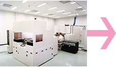 |
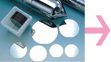
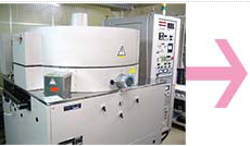
| substrate | thin film | ion implantation |
 |
 |
 |
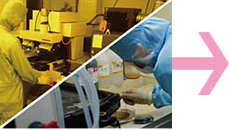
| Lithography & Etching | Chemical Mechanical Polishing | Wafer Bonding |
thin film
| type | methods, apparatuses | comment | Substrate Size |
| Insulating layer formation | thermal oxidation | ≦10µm | Φ2" to Φ300 |
| Chemical Vapor Deposition | SiO 2, PSG, NSG, etc. | Φ4"、Φ5" | |
| Low‑Pressure Chemical Vapor Deposition | polysilicon, etc. | Φ2" to Φ4", Φ6" | |
| Chemical Vapor Deposition | SiO₂, SiN, a‑Si, etc. | Φ2" to Φ8" | |
| Metal and insulating layer formation | Sputtering (PVD) | Metals, alloys, oxides, nitrides, special materials, etc. | Φ2" to Φ450, ≤650×950 |
| Evaporation | Metals, alloys, oxides, nitrides, special materials, etc. | Φ2" to Φ300, ≤300 x 360 | |
| Electroplating / Electroless plating |
Electroplating: Ni, Cu, Au, SnAg
Electroless plating: Ni, Cu, Au
|
≤Φ8", square |
patterning
|
Type
|
Methods, Equipment
|
Comments
|
Substrate Size
|
|
Photolithography Process
(Resist Coating, Exposure, Development)
|
Spin-coating
|
positive photoresist, negative photoresist
|
Φ2" to Φ8"
|
|
Contact Aligner
|
Capability: >3μm
|
Φ2" to Φ8"
|
|
|
Dual‑sided aligner (G‑line)
|
Capability: >1μm
|
Φ4"
|
|
|
Stepper (i‑line)
|
Capability: >0.5μm
|
Φ4", Φ6"
|
|
|
Nanoimprinting
|
Imprint resist (nanoscale)
|
Inquire for details
|
|
|
Electron Beam Lithography
|
Capability: >50nm
|
≤Φ6"
|
|
| lift‑off |
Lift‑off
|
Capability: >5μm
|
Φ2" to Φ8"
|
etching
| Type |
Methods, apparatus
|
Comments
|
Substrate size
|
| Dry etching |
Parallel‑plate RIE
|
Silicon etching, quartz etching
|
Φ2" to Φ8"
|
|
ICP‑RIE
|
Silicon etching, quartz etching
|
Φ4", Φ6"
|
|
|
Deep Reactive Ion Etching of Silicon
|
Si (Through‑Hole)
|
Φ2" to Φ6"
|
|
|
Sacrificial Layer Etching
|
Silicon, Silicon Dioxide
|
Φ2" to Φ6"
|
|
|
Metal Etching
|
Aluminum and Aluminum Alloys
|
Φ2" to Φ4"
|
|
| Wet Etching | Tetramethylammonium hydroxide, Potassium hydroxide | Select the appropriate | Φ2" to Φ8" |
| high‑frequency | Φ2" to Φ8" | ||
| Etching of various metal layers | Φ2" to Φ8" |
Ion implantation
|
Type
|
Method, Device
|
Comment
|
Substrate Size
|
|
Ion Implantation
|
Medium‑Current Ion Implantation
High‑Energy Ion Implantation
|
More than 60 elements can be used for doping
|
Φ3" to Φ6"
|
|
Annealing
|
High‑energy high‑speed annealing
|
Maximum heating temperature: 1800℃
|
≤Φ8"
|
bonding
|
Type
|
Method, Device
|
Comment
|
Substrate Size
|
| wafer bonding |
anodic bonding
|
bonding glass and silicon
|
≤Φ8"
|
|
Surface-activated bonding
|
Capable of bonding different materials together
|
Inquire for details
|
polishing
|
Type
|
Method, Device
|
Comment
|
Substrate Size
|
|
Wafer Bonding
|
Chemical Mechanical Polishing
|
Metals: Au, Pt, Cu, etc.
Oxides: TEOS, SiO₂, etc.
|
.Φ2" to Φ300, square
|
Analyze
|
Type
|
Method, Device
|
Comment
|
Substrate Size
|
| Surface Analysis | SIMS, ESCA, TEM, etc. | Various Contract Analysis Services | Ask for details |
| Observe the shape of a very small area under a microscope | |||
| Thermal analysis |
 customer service1