

 |
Heater
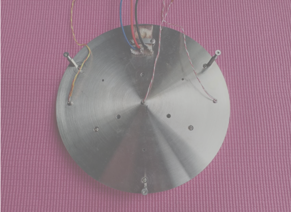
A key component of SEMI equipment for CVD and Etch processes in the manufacturing of semiconductor wafer heaters.
The core technology is to deliver uniform heat across the surface of silicon wafers when in contact with the heater.
|
CVD process


|
Main Material
|
Aluminum Al 6061
|
|
Process
|
CVD
|
|
Operating Temperature
|
120°C
|
|
Temperature Uniformity
|
±1%
|
|
Remarks
|
Brazed type. Low‑power heating element. Cooling channel
|
PVD process
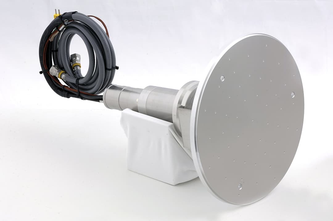
| Main Material | SST |
|
Process
|
PVD‑Semi
|
|
Operating Temperature
|
350°C
|
|
Size
|
12”
|
|
Remarks
|
12‑inch wafer heating plate‑Heating & Water Cooling
|
ASHING Process:


|
Main Material
|
Aluminum A356
|
|
Process
|
Ashing Process
|
|
Operating Temperature
|
250°C
|
|
Size
|
12”
|
|
Temperature Accuracy‑Temperature Uniformity
|
±2°C
|
|
Remarks
|
Cast type. Wafer loading on ATM. Hard anodizing
|
In the process of manufacturing semiconductor wafers, wafers are usually subjected to numerous treatments. Among them, the ashing process generally
takes place after the etching or implantation steps are performed. At this point, photoresist or other etching residues remain on the wafer, and these
residues usually need to be removed through the ashing treatment.
takes place after the etching or implantation steps are performed. At this point, photoresist or other etching residues remain on the wafer, and these
residues usually need to be removed through the ashing treatment.
Current ashing methods generally employ plasma‑enhanced ashing with oxygen‑containing gases such as O₂/N₂ to remove photoresist or carbon layers.
Since the wafer needs to be heated to 200℃‑300℃ during this treatment, the surface of the silicon substrate or bottom electrode is prone to oxidation.
Consequently, dry or wet cleaning treatment is further required to remove the oxide layer. However, such approaches will increase resistance, cause RC
delay, and thereby degrade device performance.
In addition, ashing processing tools generally have two transfer modes, namely ATM (Atmosphere Transfer Module) transfer and VTM (Vacuum Transfer
Module) transfer. When the ashing process is carried out with an ATM tool, the wafer is exposed to the atmosphere during both the temperature‑ramp‑up
process before the process and the temperature‑ramp‑down process after the process, which oxidizes the wafer surface and impairs its performance.
Module) transfer. When the ashing process is carried out with an ATM tool, the wafer is exposed to the atmosphere during both the temperature‑ramp‑up
process before the process and the temperature‑ramp‑down process after the process, which oxidizes the wafer surface and impairs its performance.
One objective of the ASHING process is to overcome at least one drawback in the prior art and provide a method for fabricating a semiconductor device,
which includes an ashing process for removing etching residues on the surface of a semiconductor substrate. This method can suppress the problem that
the substrate surface is susceptible to oxidation during temperature rise and re‑oxidation when a high‑temperature substrate comes into contact with the
atmosphere. Meanwhile, it delivers stronger residue removal capability compared with conventional ashing processes.
To achieve the above objectives, the following technical solution is provided:
A method for fabricating a semiconductor device, comprising:
providing a semiconductor substrate, which includes a patterned layer and a to‑be‑removed layer disposed on the patterned layer; removing the
to‑be‑removed layer under a vacuum state, comprising:
to‑be‑removed layer under a vacuum state, comprising:
performing a first temperature‑control process on the semiconductor substrate; performing a second temperature‑control process on the semiconductor
substrate after the first temperature‑control process; performing a cooling process on the substrate after the second temperature‑control process; wherein
removing the to‑be‑removed layer is performed under a reducing‑gas atmosphere.
substrate after the first temperature‑control process; performing a cooling process on the substrate after the second temperature‑control process; wherein
removing the to‑be‑removed layer is performed under a reducing‑gas atmosphere.
In an embodiment, the reducing gas is selected from ammonia, hydrogen, a mixture of ammonia and an inert gas, or a mixture of hydrogen and an inert gas,
and the inert gas may be nitrogen.
and the inert gas may be nitrogen.
According to one embodiment of the present disclosure, the method further comprises:
performing the first temperature‑control process at a first vacuum degree;
performing the second temperature‑control process at a second vacuum degree;
performing the cooling process at a third vacuum degree;
wherein the first vacuum degree is higher than the second vacuum degree, and the second vacuum degree is higher than the third vacuum degree.
In an embodiment, the pressure at the first vacuum degree ranges from 0 mTorr to 100 mTorr, the pressure at the second vacuum degree ranges from
600 mTorr to 1500 mTorr, and the pressure at the third vacuum degree ranges from 800 mTorr to 2000 mTorr.
600 mTorr to 1500 mTorr, and the pressure at the third vacuum degree ranges from 800 mTorr to 2000 mTorr.
In an embodiment, the temperature of the first temperature‑control process does not exceed 80℃.
In an embodiment, the second temperature‑control process includes a temperature‑ramp‑up process and a constant‑temperature process. After the substrate
reaches a temperature of 200℃‑300℃ through the temperature‑ramp‑up process, the constant‑temperature process is executed.
reaches a temperature of 200℃‑300℃ through the temperature‑ramp‑up process, the constant‑temperature process is executed.
In an embodiment, the cooling process comprises: introducing an inert gas to perform the cooling process on the substrate. The substrate temperature after the
cooling process does not exceed 60℃, and the inert gas may be nitrogen.
photolithography process
cooling process does not exceed 60℃, and the inert gas may be nitrogen.
photolithography process
|
Main Material
|
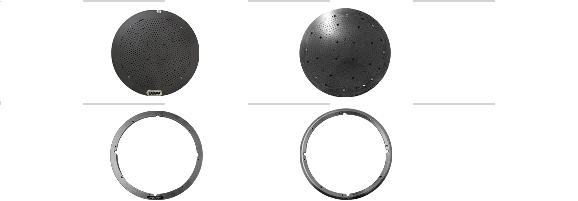
Aluminum Al 6061‑T6
|
|
Manufacturing Process
|
Photolithography
|
|
Operating Temperature
|
260°C
|
|
Wafer Size
|
12"
|
|
Remarks
|
Heating & air cooling, water cooling
|
In integrated circuit manufacturing, the size of the critical dimension (CD) is mainly determined by the lithography process. As device dimensions shrink,
lithography requires ultraviolet light with shorter wavelengths and compatible photoresists. In 248 nm and 193 nm lithography processes, when photoresist
is coated on the surface of dielectric layer materials such as silicon nitride and silicon oxynitride, the photoresist in exposed areas often cannot react completely,
forming a footing structure after development, which affects the critical dimension.
Footing is generally caused by acid‑base imbalance between the photoresist and the dielectric layer. The current solution to this problem is to first deposit an
organic bottom anti‑reflective coating (BARC) or hexamethyldisilazane (HMDS) adhesion promoter on the dielectric layer. This avoids direct contact between the
photoresist and the dielectric layer while improving anti‑reflection performance or enhancing photoresist adhesion. However, this method not only adds an extra
spin‑coating process, but also requires etching to remove BARC or HMDS after exposure, resulting in complicated processes.
 customer service1