

mechanical, electromechanical or thermodynamic means. Mineral‑insulated heating elements from Fullchance find wide‑ranging applications in
deposition systems.
What is Chemical Vapor Deposition (CVD)?
Chemical Vapor Deposition is a vacuum thin‑film deposition process that employs thermally induced chemical reactions on the surface of a substrate.
The process varies slightly depending on the materials used.
The process varies slightly depending on the materials used.
• When the coating is a metal or alloy, it is evaporated via heating or pressure changes. The vapor then deposits onto the cooler semiconductor wafer
(substrate) to form a uniform coating.
(substrate) to form a uniform coating.
• When the coating is a polymer (e.g. silicon nitride), two or more gaseous precursors (monomers) are decomposed by heat. They then react with one
another inside a vacuum chamber to form new polymer compounds, which deposit onto the substrate as a thin‑film layer.
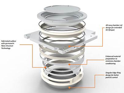
Adjustments to pressure, temperature, and duration influence the thickness of deposited layers. In fact, there are many sub‑categories of CVD processes
depending on these variables. These include:
another inside a vacuum chamber to form new polymer compounds, which deposit onto the substrate as a thin‑film layer.
Adjustments to pressure, temperature, and duration influence the thickness of deposited layers. In fact, there are many sub‑categories of CVD processes
depending on these variables. These include:
• Atmospheric‑Pressure Chemical Vapor Deposition (APCVD): Thermally driven at atmospheric pressure with a high deposition rate. Extremely high
temperatures between 1000 °C and 1300 °C are required.
temperatures between 1000 °C and 1300 °C are required.
• Low‑Pressure Chemical Vapor Deposition (LPCVD): Uses low pressure and heat to react precursor gases on a solid substrate. Reduced pressure minimizes
unwanted gas‑phase reactions and improves thin‑film uniformity on semiconductor wafers. The temperature typically ranges from 570 °C to 650 °C.
unwanted gas‑phase reactions and improves thin‑film uniformity on semiconductor wafers. The temperature typically ranges from 570 °C to 650 °C.
• Ultra‑High‑Vacuum Chemical Vapor Deposition (UHCVD): Performed at very low pressure, generally below 10⁻⁶ Pa.
• Plasma‑Enhanced Chemical Vapor Deposition (PECVD): A low‑temperature (and thus more cost‑effective) thin‑film deposition process. It operates at
temperatures ranging from 100 °C to 400 °C. Cold plasma is introduced along with reactive gases to form the desired coating on the substrate.
temperatures ranging from 100 °C to 400 °C. Cold plasma is introduced along with reactive gases to form the desired coating on the substrate.
• Photo‑Initiated Chemical Vapor Deposition (PICVD): Uses ultraviolet light to excite chemical reactions. It is similar to PECVD because plasma is a strong
emitter of ultraviolet radiation. Under certain conditions, PICVD can operate at or near atmospheric pressure.
emitter of ultraviolet radiation. Under certain conditions, PICVD can operate at or near atmospheric pressure.
• Atomic Layer Deposition (ALD): Employs multiple alternating gases. Each gas reacts with and saturates the substrate surface. The chamber is then purged
with inert gas before another reactive gas is admitted to form the next deposited layer. This technique is also applied in nanotechnology.
What are the advantages and disadvantages of CVD?
with inert gas before another reactive gas is admitted to form the next deposited layer. This technique is also applied in nanotechnology.
What are the advantages and disadvantages of CVD?
CVD can be used to form thin‑film layers on a variety of materials such as glass, ceramics, metals and metal alloys at fairly high deposition rates. The advantage
of CVD over Physical Vapor Deposition (PVD) is that it can be used to form uniform coatings even on complex shapes. In fact, this feature, combined with the high
purity of CVD deposits, makes it very useful in sensitive nanotechnology processes. Impurities can be easily removed from gaseous precursors during chemical
vapor deposition. This is another advantage for nanotechnology applications.
On the downside, CVD precursors can be highly toxic, explosive or corrosive, and residual products constitute hazardous waste. In addition, some precursors may
be expensive.
be expensive.
What heating solutions does Fullchance provide for CVD processes?
There are various heating methods for CVD coating applications, and resistive heating is one of the most important and widely‑used approaches. This is an area of
expertise for Fullchance , which offers a range of high‑quality mineral‑insulated heating elements well‑suited for CVD applications. Micro heaters represent another example
of custom‑designed heating solutions for CVD.
expertise for Fullchance , which offers a range of high‑quality mineral‑insulated heating elements well‑suited for CVD applications. Micro heaters represent another example
of custom‑designed heating solutions for CVD.
As nanotechnology adopts CVD, thermal performance is critical for controlling thin‑film deposition and ensuring quality. At St. Berlin, we possess the expertise to design
custom heating systems that address the challenges posed by all kinds of CVD processes. Our high‑temperature precision heaters can be combined with advanced
temperature sensors to guarantee the thermal uniformity vital to these processes.
custom heating systems that address the challenges posed by all kinds of CVD processes. Our high‑temperature precision heaters can be combined with advanced
temperature sensors to guarantee the thermal uniformity vital to these processes.
Advantages of Mineral‑Insulated Heating Elements for CVD
• Temperatures up to 1000°C
• Mineral insulation ensures
◦ Heating elements are suitable for demanding atmospheres (vacuum, inert gas)
◦ Chemical resistance
◦ Excellent dielectric durability
• Customizable sheath materials to suit any environment
• Seamless transition between hot and cold sections of the heater
• Equal diameters for hot and cold sections
• Simple termination as cold ends prevent overheating
• Suitable for high power density
• Uniform heat distribution across sources, wafers, targets or substrates
• Large bend radius enables heating elements for complex bending applications
• Precise heating for critical processes
• Thinner and lighter designs are feasible
• Fast warm‑up time
• Sealed heating elements prevent contamination
• Thermocouples can be integrated into the design
You can read more about our work in the semiconductor industry here.
 customer service1